Sunday, March 30, 2014

Microchiping - Light Up An LED

Basically there are two ways to drive a LED using a microcontroller:

  • using direct drive (when the current needed by the LED is less then the maximum rated current of the digital I/O pin and the application doesn't need a stable light intensity).
  • using an external driver circuit (like a current source - when you need more precision/constant light intensity).


Direct Drive

In this case you connect the LED directly to the digital I/O pin, together with a current limiting resistor. The value of the resistor can be computed using formula (1), after you know the Vf (forward voltage) and If (forward current) of the LED (this values can be found in the datasheet).

R = (Vdd - Vf) / If     (1)

Our circuits Vdd is 5 V and the LED has a Vf of 3.3 V (typical) at If = 20 mA. The series resistor computed value is 85 Ω.

LED Datasheet Example

In the following schematic LED1 will light-up when the output pin value is '1' and LED2 will light-up when the output pin value is '0'.

Direct Drive Connection

If you want to drive more then a single LED, you will need more current (if you connect the LEDs in parallel) or more voltage (if you connect the LEDs in series). Probably this will exceed the capabilities of the microcontroller, so you'll need to use an external drive circuit (as simple as an transistor).

The code example will blink the two LEDs. Pay attention the way LED2 is light-up (by clearing the value of the associated bit from LATA register).

   void main(void) {

      // internal oscillator configuration
      // use INTOSC with Fosc = 8MHz
      OSCCON = 0x73;

      // ports configuration
      // bits 0 and 1 of port A configured as digital I/O
      ANSELA &= 0xFC;
      // bits 0 and 1 of port A configured as digital outputs
      TRISA &= 0xFC;
      // LEDs off - LATA.B0 = 0, LATA.B1 = 1
      LATA = 0x02;

      // endless loop
      // change the state of the LEDs every 1 second
      while(1) {

         Delay_ms(1000);   // wait 1 s (1000 ms)
         LATA = 0x01;      // turn on LEDs
         Delay_ms(1000);   // wait 1 s (1000 ms)
         LATA = 0x02;      // turn off LEDs

      }

   }

Note: code developed using <MikroC PRO for PIC>. For more information about MikroC IDE go to the dedicated article.


External Driver Circuit

External drivers are used in two scenarios: when you have to switch on more than one LED using a single uC output pin or when you need an exact light intensity.

To drive a group of LEDs using one single digital output you need a semiconductor switch (a transistor) and a power supply. For example if you have n LEDs connected in series the formula (2) for R and the schematic are presented below:

R = (Vext - (n Vf + 0.2)) / If,     (2)

                              n -number of LEDs
                              0.2 - voltage drop on transistor

Driving n LEDs Using One Single Digital Output Pin

Light intensity is directly dependent on the current that flows trough the LED. That makes current sources the best drivers for LEDs.

The next schematic contains a simple current source powering a LED.

Driving LEDs Using A Current Source

One single digital pin required to switch the LED on and off. Value of R is computed with formula (3).

R = 0.6 / If     (3)

Monday, March 24, 2014

Microchiping - I/O Ports

I/O ports are the interface between the uC and the outside world. Every pin of a port can be configured as a digital input/output. Some of them can also be configured as analog inputs.

There are 4 registers used to configure and control I/O ports on PIC16F1938:
  • TRISx Register - Sets up the direction of the port pins;
  • PORTx Register - Used for reading the values of the port pins;
  • LATx Register - Used to set the values of the port pins;
  • ANSELx Register - Sets up the analog/digital function for port pins.
Note: The 'x' from every register name should be replaced with the corresponding letter!


Set up the port direction - TRISx Register

Setting a TRISx bit will make the corresponding pin an input and clearing a bit from the TRISx register will make the corresponding pin an output. To remember it easier I use the following association:
  • 1 - 'i' - input.
  • 0 - 'o' - output.

If you want to set the pins 0, 3 and 4 of the port B (8 bit port) as inputs and the rest of them as outputs you will write the following code line:

   TRISB = 0b00011001;


Reading the port value - PORTx Register

The port pins are set up as inputs. How do you read the value of the port?! You simply read the value of the associated PORTx register.

Let's say the logic levels on pins 2, 3 and 6 are high and the others are low. The value of the port will be 0b01001100 (76 - decimal). The next code lines will run until the value of the port will be greater then 100:

   while(PORTC <= 100) {

      valueSum = PORTC;
      counter++;

   }

You can also read the value of one single pin by using the name of the corresponding bit. For example if you only need to execute some code if the logic level on pin 5 is high:

   if(PORTA.B5 == 1) {

      // code to run

   }


Setting the port value - LATx Register

Your port is set up as output. To set the logic levels on the port bits you only need to write the apropriate value on the associated LATx register.

For example if you need high output levels on pins 7, 6 and 4, value of the LATx register will be 0b11010000 (208 - decimal).

   LATB = 0b11010000;

If you only need to set up the output level of one single pin, use the corresponding bit:

   LATB.B2 = 1;


Enabling/disabling analog function of the port - ANSELx Register

Setting a bit in the ANSELx register will assign the corresponding pin as analog input and will disable the digital input buffer.

Clearing a bit in the ANSELx register will make the corresponding pin function as a digital I/O.

If the pins 0 and 1 need to be configured as analog inputs and the rest of the port as digital I/O, register ANSELx gets the following value:

   ANSELA = 0b00000011;

Microchiping - Internal Oscillator Setup

PIC16F1938 has a configurable internal oscillator module (31 kHz - 32 MHz). Setting it up is a very simple task, involving one single register, except the case you need a 32 MHz Fosc.

PIC16F1938 - Oscilator Module
PIC16F1938 - Oscilator Module (1)

OSCCON register must be altered to setup the internal oscillator.
If SCS<1:0> bits are 10 or 11 the system clock uses the internal oscillator block. Bits IRCF<3:0> are used to select the oscillator frequency.

OSCCON Register
OSCCON Register (1)

For example the function used to initialize the internal oscillator module at a frequency of 16 MHz will look like this:

   void InitIntOsc(void) {
     
      // system clock uses the internal oscillator (SCS<1:0> = 11)
      OSCCON |= 0x03;
      // set the frequency to 16 MHz
      OSCCON |= 0x78;

   }  


(1) PIC16(L)F1938/9 Datasheet - PDF!

Microchiping - Mandatory Circuits

The PIC16F1938 can't be used without the following circuits:
  • stabilized power supply;
  • reset circuit;
  • oscillator;
  • ICSP (in circuit serial programming) connector.


Stabilized Power Supply

Usually the microcontroller circuits draw a limited amount of current from the power supply. That makes the linear regulators like 780x series or LM1117 series the logical choice for powering this applications.

The simplest fixed regulator configuration:

7805 Stabilized Power Supply

To the base configuration you can add protection circuits (overvoltage, reverse polarity) or visual indicators (like a LED). The next image displays the 7805 stabilized power supply with protection circuits and visual indicator.

7805 Stabilized Power Supply With Protection Circuits And Visual Indicator

Diode D1 is used as a reverse polarity protection. It is a Schottky diode with a rated forward current greater then the maximum current generated by the regulator. The forward voltage should be as low as possible to increase the efficiency of the supply.
D2 is a Zener diode used to protect the circuit from overvoltage. The rated voltage of the diode should be less then the maximum input voltage of the regulator circuit.
LED1 indicates that the circuit is powered. R1 resistor is used to limit the current trough the LED.

Note: All the protection circuits are the simplest possible. For more information check out the dedicated article.


Reset Circuit

All microcontrollers (or at least most of them) have a master clear reset pin. Microchip names this pin MCLR and usually uses inverted logic to drive it (to keep the uC in the reset state you should apply a logic '0' to this pin).

The recommended reset circuit is presented in the next picture:

Reset Circuit
Reset Circuit

R3 is a pull-up resistor that powers the pin. It's value is usually 10 kΩ for uC powered with 5V.
R2 protects the pin by limiting the current to a safe value (<25mA).
Capacitor C5 eliminates the transient voltages (voltage spikes). A value of 100 nF is commonly used.

A push-button can be used if you need a external reset. By pressing the button the pin is brought in a low state, resetting the uC.

Reset Circuit With Push-Button For External Reset


Oscillator

Every microcontroller needs an oscillator to generate the device clock, required for the device to execute instructions and for peripherals to function.

Usually you can select a internal or external oscillator. The internal oscillator is cheaper and doesn't consume any space on the board, but it's less accurate and stable then the external ones. 

The most used external oscillator circuit is made out of a quartz crystal and two capacitors:

External Quartz Crystal Oscillator

The two capacitors are used to increase the frequency stability. The values should be between 20 pF and 32 pF, and equal.

Some uC have internal oscillators with frequencies up to 32 MHz. The setup process of a internal oscillator is described into the dedicated article.


ICSP (in circuit serial programming) Connector

The standard connector for Microchip ICSP is the following:

ICSP
ICSP

This interface allows the user to upload the code (.hex file) from the PC to the uC using a programmer device like Pickit, MPLAB ICD or others.

MCLR connects to the uC's reset pin.
Vdd and Vss are are connected to the power and ground pins.
PGD stands for "Programming Data" and must be connected to the corespondent pin on the uC. It can also be named ICSPDAT.
The programming clock (PGC) can also be named ICSPCLK.
The PGD and PGC signals are preferably routed directly to the microcontroller pins, without using other circuit elements.

Tuesday, March 4, 2014

EAGLE CAD - Automatic Rename All The Components Inside A Schematic

While you're working at a schematic is hard to keep all the component names in order, but at the end it would be nice and helpful if they were. To do this manually it's out of discussion, so we need an automated way to do it. That's why'll be using a User Language Program.

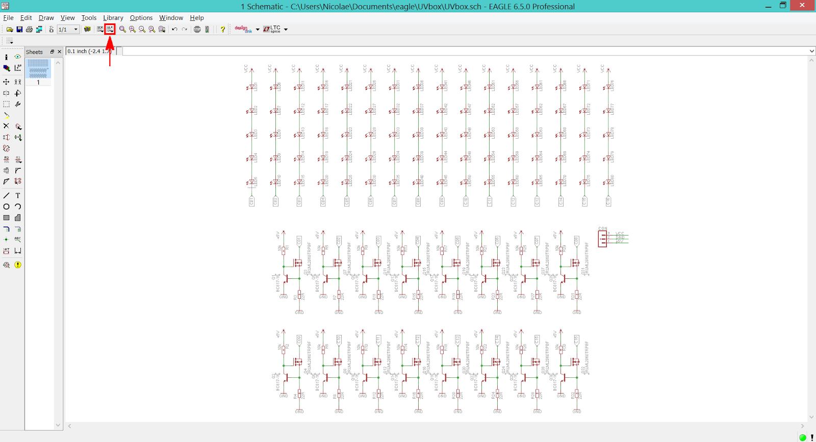
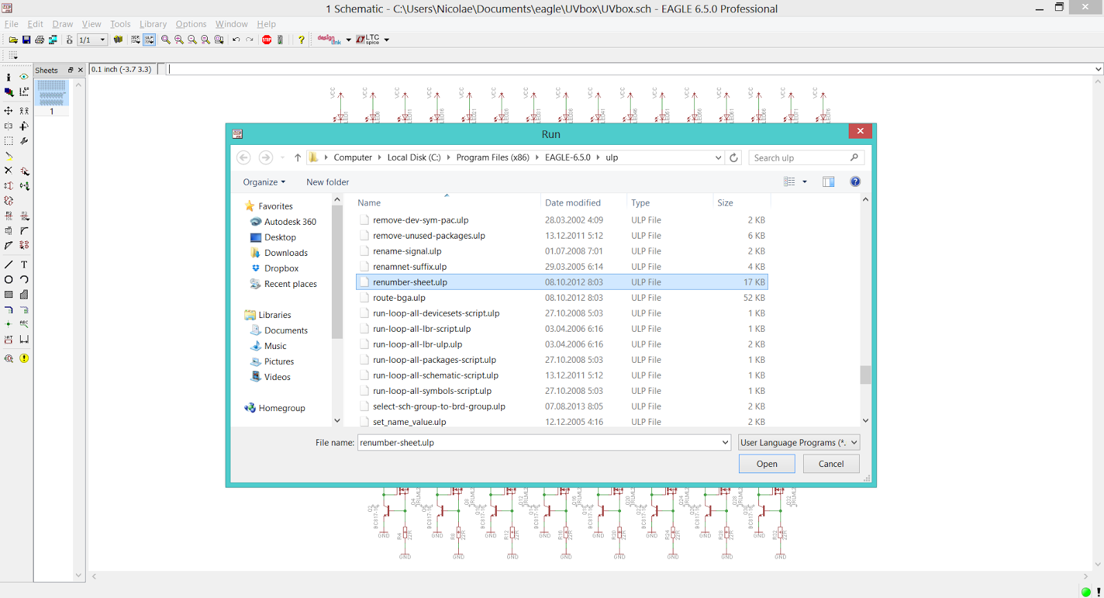
When you're done with you're schematic press the ULP button from the Toolbar and inside the opened window search for the renumber-sheet.ulp file.

EAGLE CAD - ULP Button, Located On The Toolbar

EAGLE CAD - Open The renumber-sheet.ulp Script

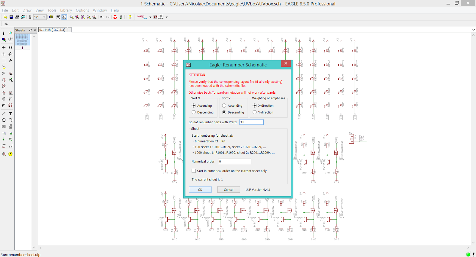
You have a couple of options to play with, after what you'll press the OK button to run the script. Simple as that!

EAGLE CAD - Press The OK Button To Run The Script

EAGLE CAD - Save a schematic/board as PDF file

To do that just press the Print button or follow the path File > Print. The Print window appears. On the Printer field chose the Print to File (PDF) option.

EAGLE CAD - How To Save Your File As PDF

Monday, March 3, 2014

EAGLE CAD - Creating Transparency Films From The Board Editor

We just finished our Board schematic in Eagle. What now? Well... we're moving to the real world by creating the transparency films used to manufacture the PCB's.

In the Board Editor select the Layer settings button. The Display window appears. Click on the None button to deselect all the layers.

Click the Layer settings button

Click the None button to deselect all the layers

To create the bottom filter select the following layers:

  • 16 Bottom
  • 17 Pads
  • 18 Vias
  • 20 Dimension
  • 45 Holes

The Circuit Board Ready For Printing The Bottom Layer Transparency Filter

Click on the Print button or follow the path File > Print. The Print window appears. After selecting the printer, paper type, orientation and alignment, set the area to full. The scale factor and page limit should be 1. In the Options area just the Black and Solid options should be checked. Set the Calibrate values to 1 and the Border values to 10.

Printer Settings For The Bottom Layer

Go one... you're ready to print the transparency film for the bottom layer. Click the OK button.

For the top filter you should select the following layers:
  • 1 Top
  • 17 Pads
  • 18 Vias
  • 20 Dimension
  • 45 Holes

The Circuit Board Ready For Printing The Top Layer Transparency Filter

The printer setting are the same as to the bottom layer, but in the Options area you also should check the Mirror option.

Printer Settings For The Top Layer

Now you can print the transparency film for the top layer too. For information about how you can make a real PCB using the transparency films you just printed, read this.

How To Make A PCB (Printed Circuit Board) - WORK IN PROGRESS

There are a lot of methods used for PCB manufacturing, but for the everyday hobbyist two of them step up in terms of accessibility and quality: making PCB's by photo-etching method and by milling (with a CNC).

This will be about the photo-etching method. Why? Simply because it allows you to create double-sided PCB at a high quality using easy accessible materials.

What do you need?

  • PCB Design Software (yes, like Eagle CAD).
  • One printer - after some years of testing I've settled down with a simple inkjet printer (higher printing resolution is better) .
  • Transparency film - A4 sheets, no matter what brand as long as it is compatible with your printer (one example is the HP Premium Inkjet Transparency Film).
  • Photoresist PCB's - you can make your own but it's no worth. You can find everywhere PCB's already covered with photoresist (Bungard Elektronik is one of the greatest manufacturers in this area).
  • Sodium Hydroxide (NaOH) for etching the photoresist. Special care is required to prepare the solution: 7 grams NaOH for every liter of water (H2O).
  • Ferric Clorhidre (FeCl3) for etching the cooper. You can buy it directly as a solution.
  • One UV light source. I use a DIY UVbox which will be discussed in another article.

Additional materials are needed if you plan to make double-sided PCB's, solder masks, silk layers, ...

To create the PCB you need to go trough the following steps:

     1. Create the circuit schematic (using the PCB Design Software).
     2. Based on the schematic, create the board/layout (also using the PCB Design Software).
     3. Print the transparencies for every layer of the board (bottom, top and bottom). Pay special attention on printing the top layer - it has to be mirrored! 
     4. If you are going double-side, align the two layers.
     5. Make a sandwich out of the transparency films and the photoresist PCB. Expose every side of it to UV light. The exposing time depends on the light source. You'll have to make some experiments first.
     6. Etch the exposed photoresist by emerging the board in NaOH solution.
     7. Wash the board with clean water and dry it. Pay special attention not to scratch the photoresist traces.
     8. Etch the exposed cooper by emerging the board in FeCl3 solution. Ideal results are obtained at a temperature of 60C.
     9. Wash the board and solder the components - the simplest PCB. If you're going the hard way you still have to apply the solder mask, silk layer or to solder the vias.

EAGLE CAD - How To Copy A Symbol From A Library To Another

First of all open the library that contains the symbol you need (from Control Panel window follow the path File > Open > Library). Click on the Symbol Tool located on the toolbar of the Library window you just opened. This will open the Edit window where you will locate and double-click the desired symbol, which will be opened in the library window.

EAGLE CAD - Double-click The Desired Symbol From The Edit Window

Select all the components of the symbol using the Group Tool.

EAGLE CAD - Select The Entire Symbol Using The Group Tool

Click on the Copy Tool and right-click on the symbol. In the pop-up menu that appears select the Copy Group option.

EAGLE CAD - Copy The Entire Group

Now close this library and open the library in which you need the symbol.
Click the Symbol Tool and insert the name of the symbol inside the Edit field. Click the OK button. On the Warning message click Yes.

EAGLE CAD - Insert The Name Of The Symbol Into The Edit Field

EAGLE CAD - Click the Yes Button On The Warning Mesage

What you still have to do is to simply paste the copied symbol using the Paste Tool. Place the symbol wherever you want on the workspace and save it (CTRL + S).

EAGLE CAD - The Symbol Is Pasted Into The New Library

Your new symbol is ready to use!

EAGLE CAD - How To Copy A Package From A Library To Another

For start open the library in which you wish to have the package (File > Open > Library).

EAGLE CAD - Open The Target Library

Go to the Control Panel window and expand the Libraries folder (left side of the window). Locate the library that contains the package you need and expand it. By experience I will say that the libraries
ref-packages.lbr and ref-packages-longpad.lbr will do 90% of the work. You can find here almost every package you need. Find the package you need and right-click it. On the pop-up menu select Copy to library. This will copy the selected package to the opened library.

EAGLE CAD - Copy The Desired Package To The Target Library

Now the package is available in the desired library.

EAGLE CAD - Bigger Pads

A bigger pad makes the solder process more comfortable. But to manually modify every pad in every library you use it's not such a practical approach. What can we do?! The answer is as simple as changing some settings!

In the Board Editor window follow this path: Tools > DRC. In the window that appears select the Restring tab. As you can see, the default value for pads diameter is minimum 10 mil. By changing this value (increasing it) you can obtain bigger pads. Use 20 mil and click the Apply button. Voilà! You doubled the diameter of all pads contained into this board file.

EAGLE CAD - Change Pads Dimension

EAGLE CAD - Enable The Grid

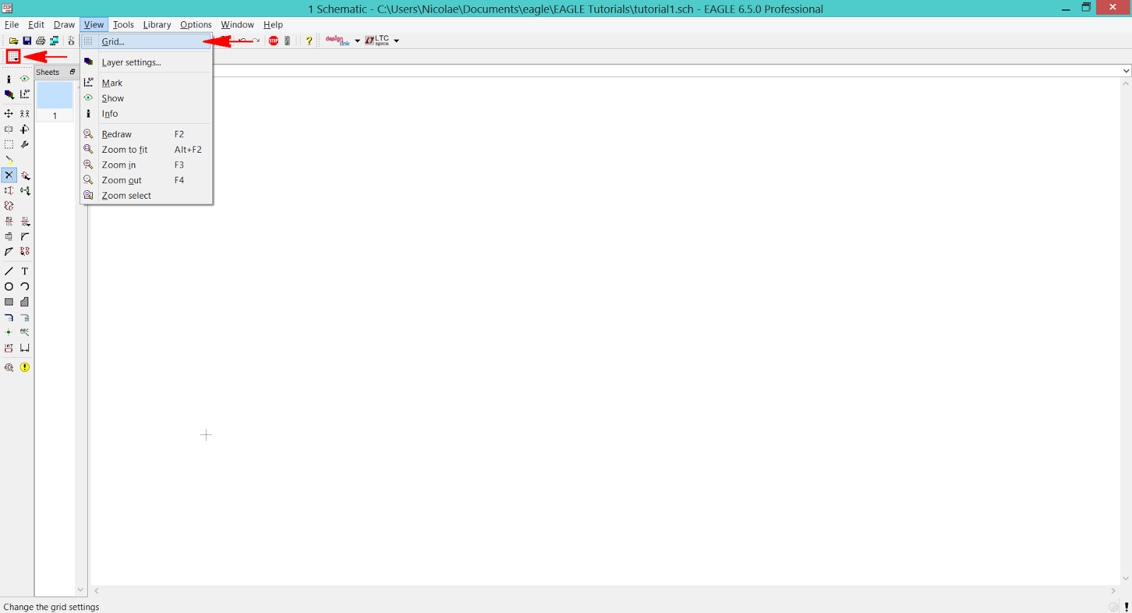
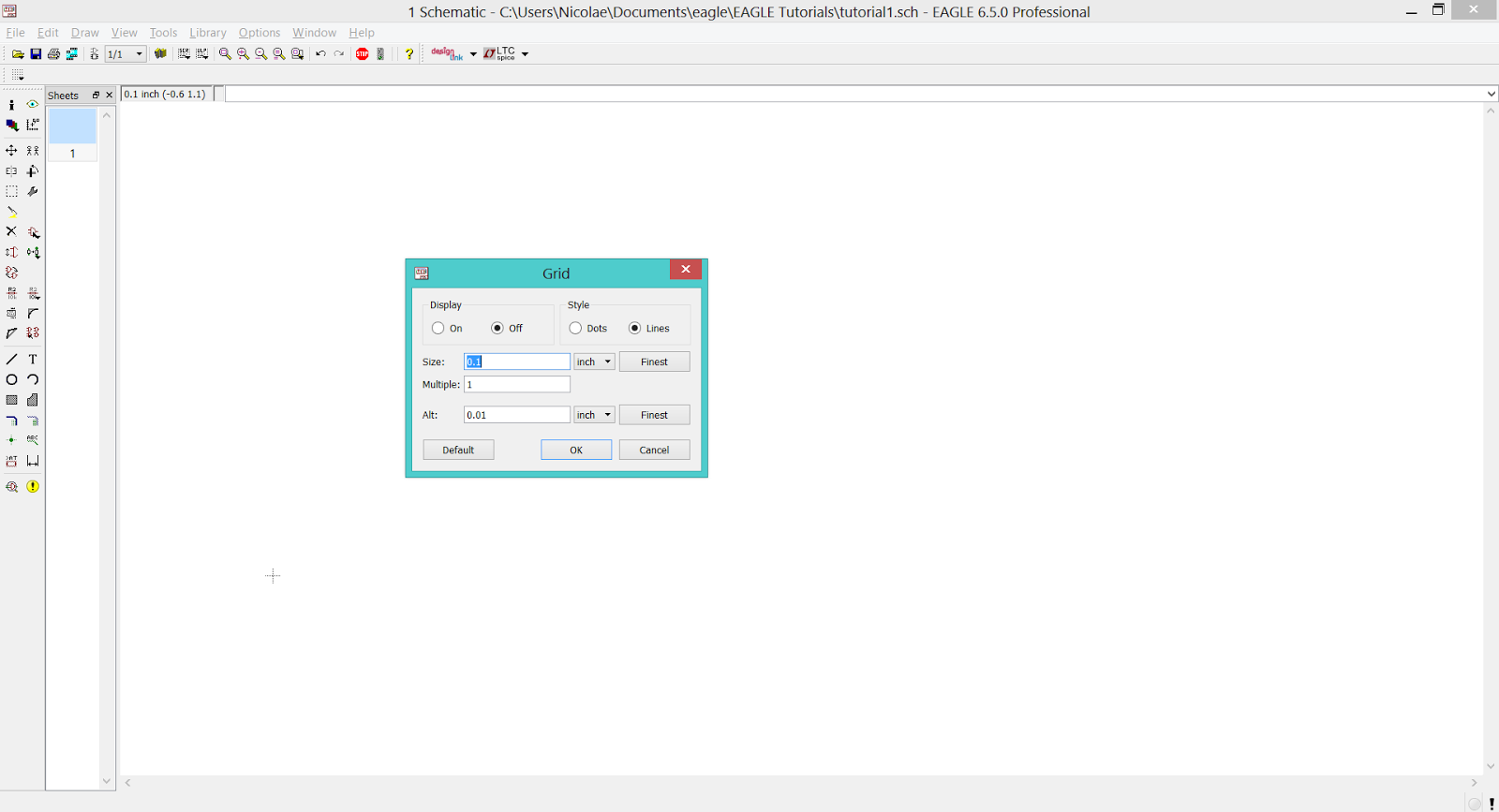
You can put a grid on the screen, both in the schematic and board editor. To do this simply follow the path View > Grid or push the dedicated button placed on the left-top of the editor window.

EAGLE CAD - Access The Grid
EAGLE CAD - Access The Grid 
The Grid window appears and allows you to display the grid or not, to select the style of the grid (dots or lines) and the size (value and units).

EAGLE CAD - The Grid Window

EAGLE CAD - Create A Custom Device

A custom library is useless if empty. So... to populate the library we have to create new devices.

Every device contains a symbol (in schematic view) and a package (in board view). In order to create the new device we should first create the symbol and the package and then combine them into one brand new and ready to use electronic part. A step-by-step guide of this process is presented in the following video:

(video - coming soon)

EAGLE CAD - Create A Custom Library

To create a new library go to the Control Panel window and follow this path: File > New > Library.

EAGLE CAD - Create A New Library

EAGLE CAD - New Library Window

If everything is OK the Library window will appear. Personally I recommend to save the custom libraries under the same folder with your personal Eagle projects (on a Windows machine the default folder is c:\...\MyDocuments\Eagle). Simply create a Libraries folder where you can save all your custom work.

You can use this custom library in you project by following the instructions in this tutorial.

Information about how to create a custom device can be found here.

Sunday, March 2, 2014

EAGLE CAD - Completing The Board

At this moment we have only a board file with all the devices footprints and highlighted connections inside. To finish the board we have to put every footprint in a position we find useful and replace the airwires with actual traces.

Before we start keep in mind one thing: the traces can be routed (with Route Tool) on both layers of the board: top (red) or bottom (blue).

So... using the Move Tool we place every device in the right place:

EAGLE CAD - Arrange Every Component On The Board In The Right Place

Then we use the Route Tool to create the actual traces, connecting the terminals/pins highlighted by airwires.

EAGLE CAD - Board With Routed Signals

EAGLE CAD - Tools Used In The Board Editor

Beside the tools that we have in the Schematic Editor, Board Editor comes with a couple of his own:

Route - used to create a signal trace between two or more terminals/pins.

Ripup - deletes the traces between terminals/pins.

Polygon - used to create signal planes.

Via - useful for jumping with a trace from a layer to another.

Hole - used for making holes in the board.

EAGLE CAD - Create A New Board

After you're done with the schematic of your circuit simply jump to the next step - creating the board.

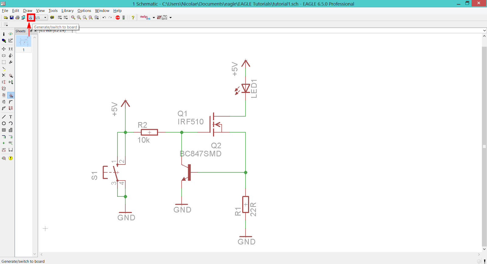
The easiest way to create the board is by pressing the Generate/switch to board button, located on the upper toolbar of the Schematic Editor.

EAGLE CAD - Create a Board File from existing Schematic File
EAGLE CAD - Create a Board File from existing Schematic File 

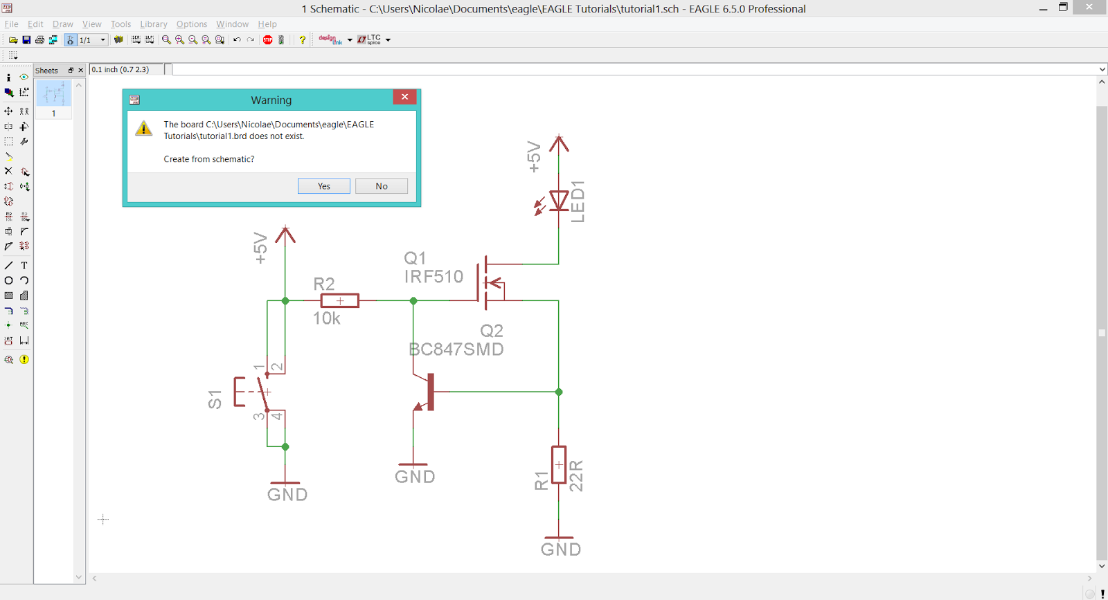
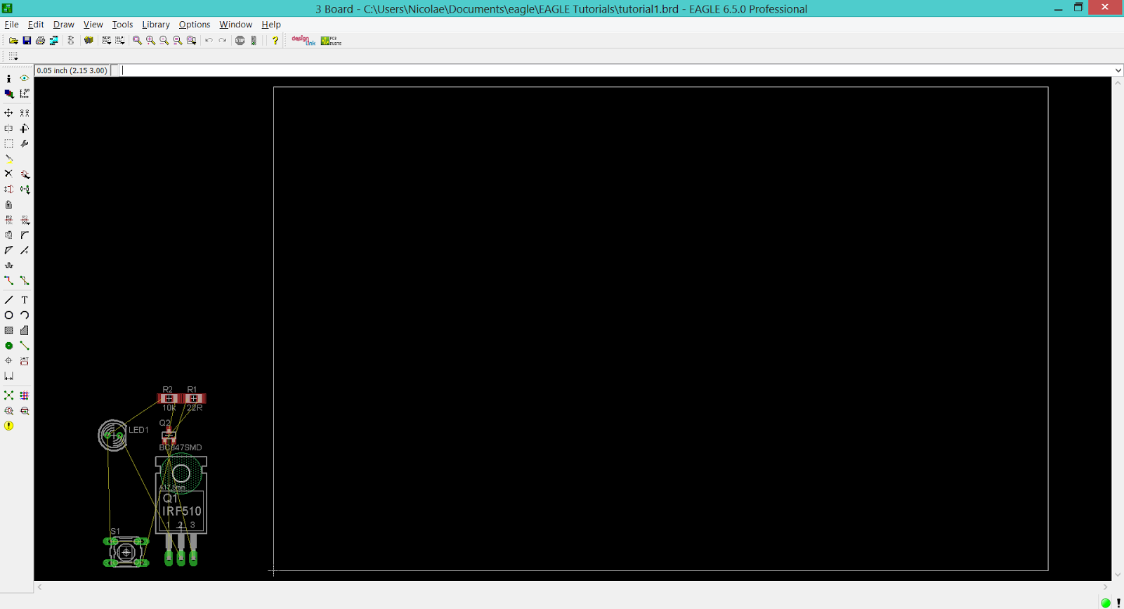
A warning message tells you that the board associated with this schematic doesn't exist and asks for permission to create it. After you click on the Yes button a new Board window opens. This board contains the footprints of all devices included in the schematic file and highlights (using thin yellow lines named airwires) the connections that have to be routed.

EAGLE CAD - Warning Message On Creating A New Board

EAGLE CAD - New Board File Based On A Existing Schematic File

EAGLE CAD - Let's Make A Real Schematic

Just to make use of and to accommodate with the Schematic Editor we'll be sketching a simple circuit. This circuit is used to power a LED with constant current.

What do we need:

  • 1 x LED (THT, 5mm type).
  • 2 x resistors (SMD 1206).
  • 1 x N channel MOSFET (IRF510, TO220 package).
  • 1 x NPN transistor (BC847, SOT23 SMT package).
  • 1 x push-button switch (Omron 10-xx type).

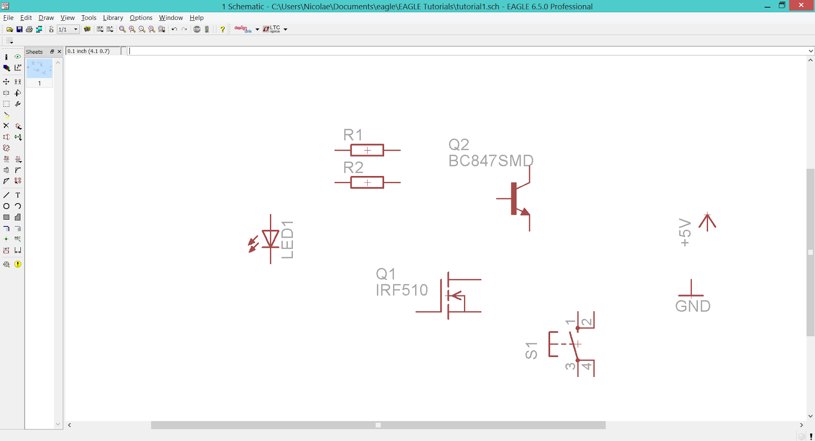
Let's open the previewesly created schematic file and start adding the components by selecting the Add Tool from the Tool Panel. This action will open the Add window.

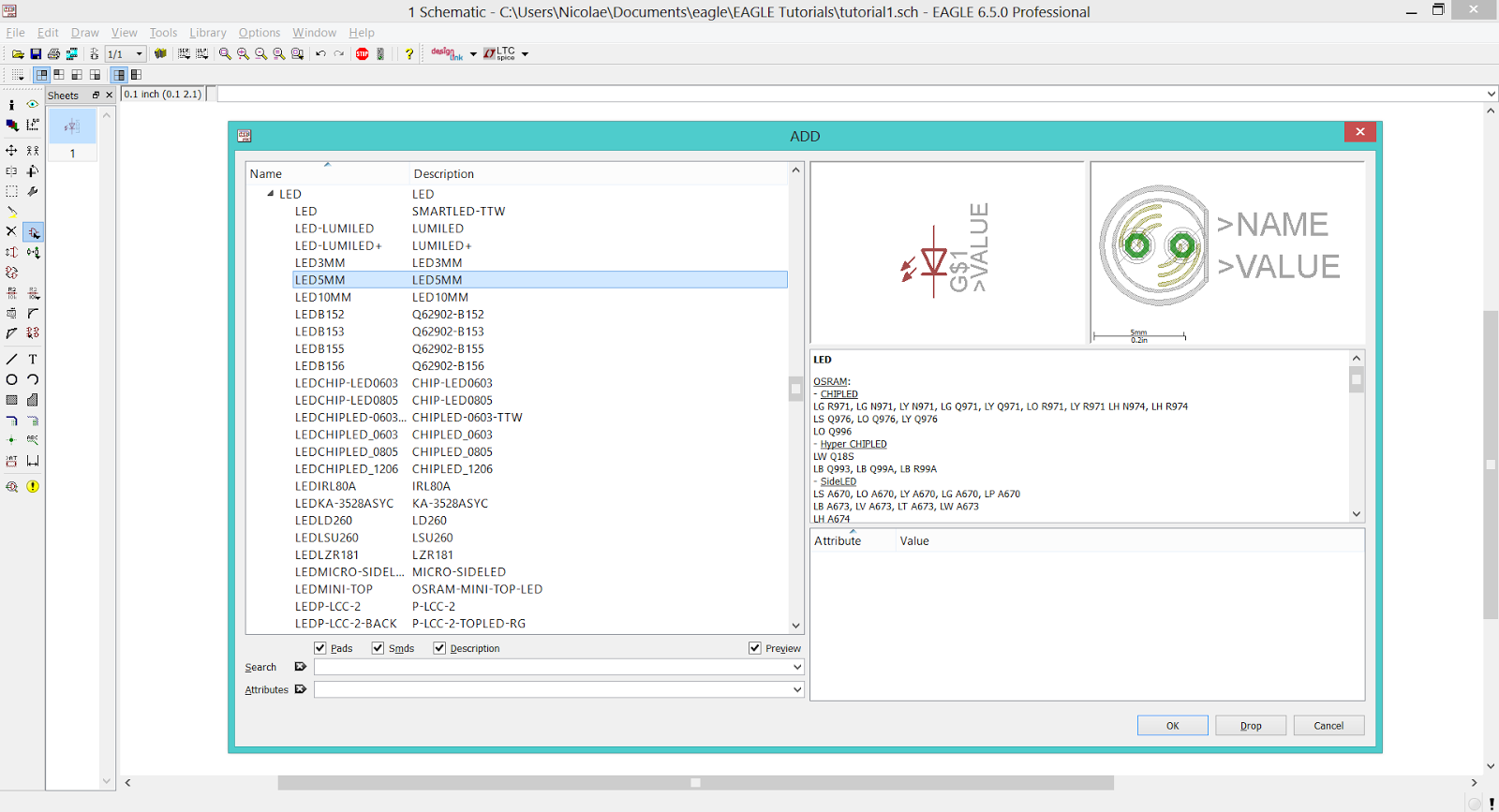
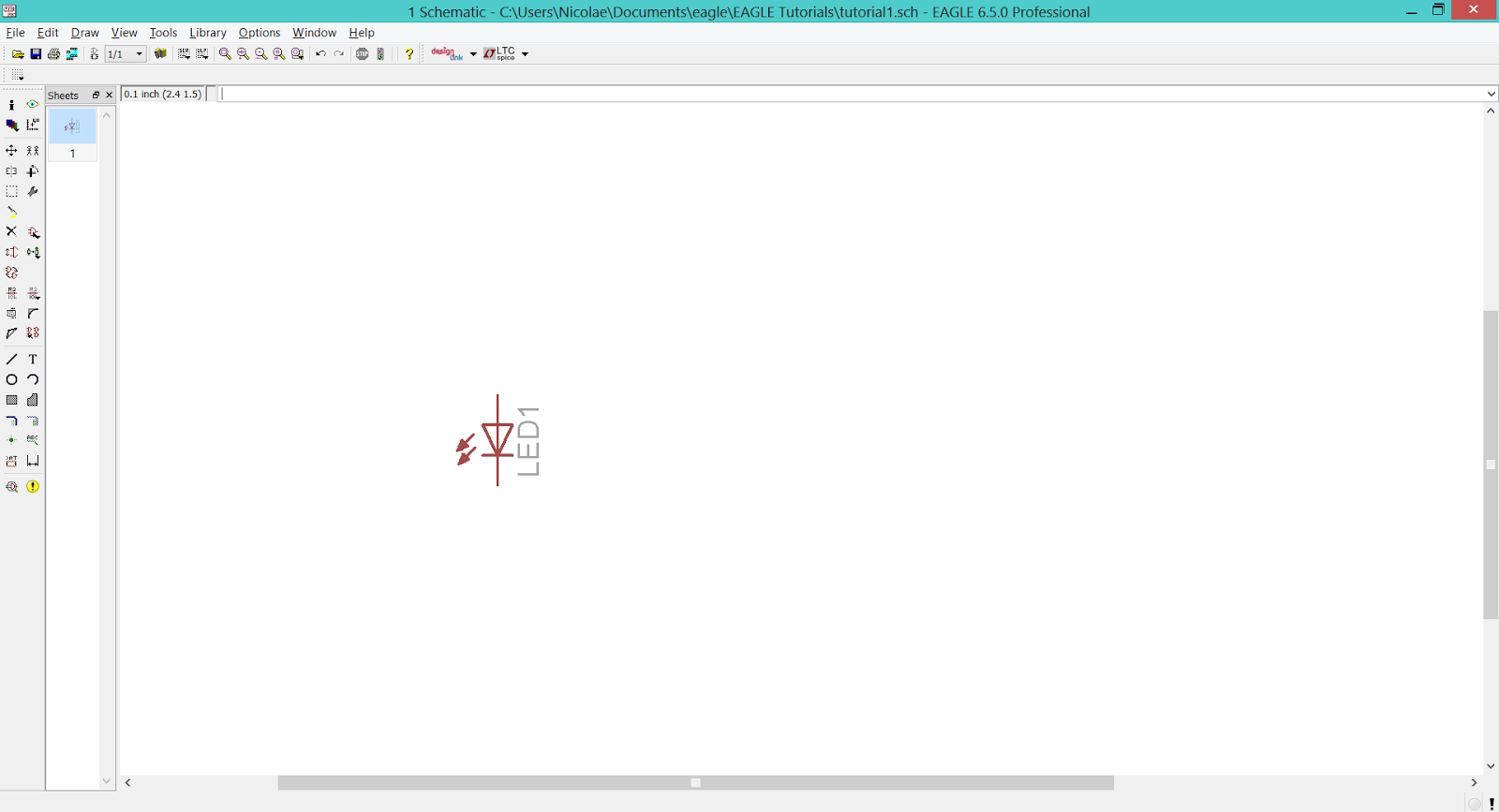
Scroll down to the LED.lbr library, expand it and in the LED option you will find the LED5mm - the device that we need, and place it on the workspace.

EAGLE CAD - LED Library

EAGLE CAD - Placing The LED

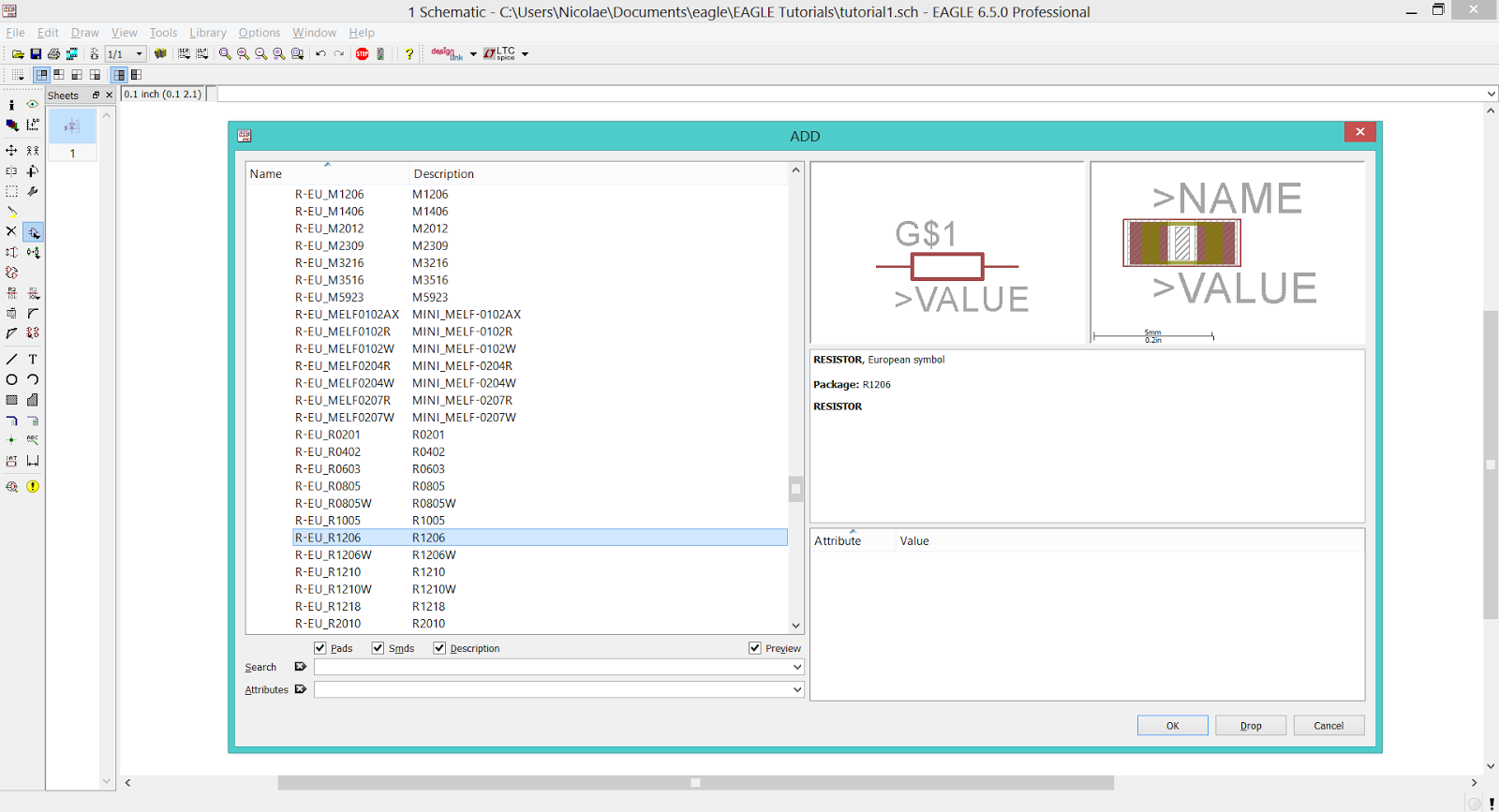
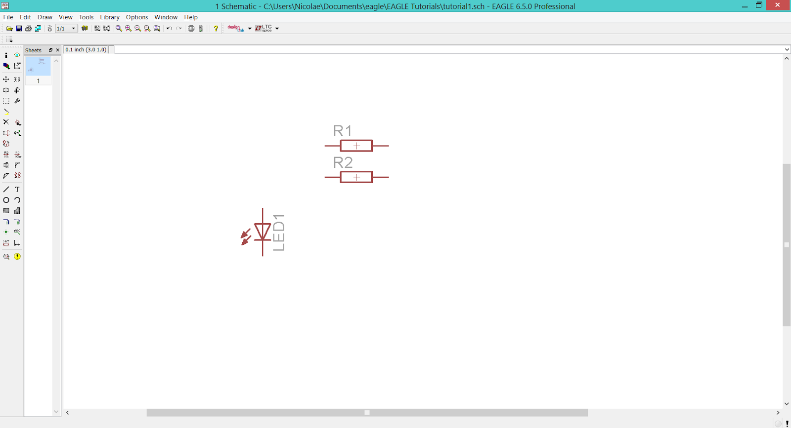
Return to the Add window and follow the next path: rcl.lbr > R-EU_ > R-EU_R1206. This is the R1206 SMD resistor that we need. Place two of them on the workspace and return to the Add window.

EAGLE CAD - RCL Library

EAGLE CAD - Placing The Resistors

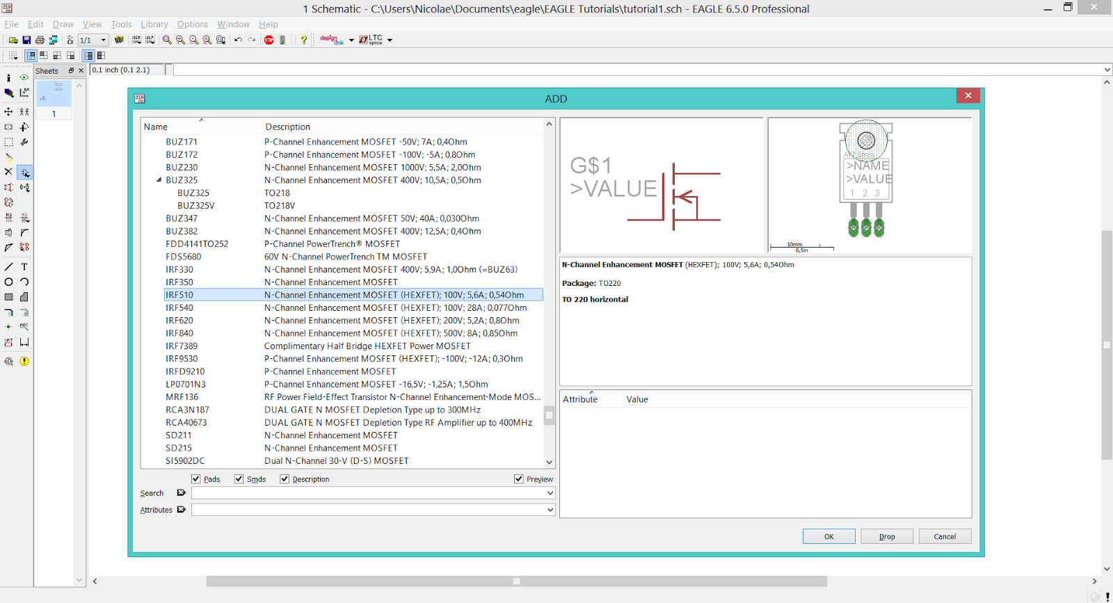
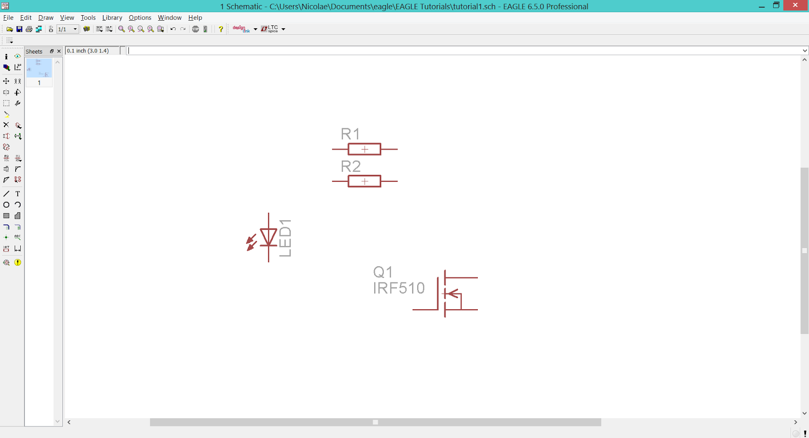
To add the N channel MOSFET go to transistor-fet.lbr > IRF510. Add one on the workspace.

EAGLE CAD - Transistor-FET Library

EAGLE CAD - Placing The N-MOS Transistor

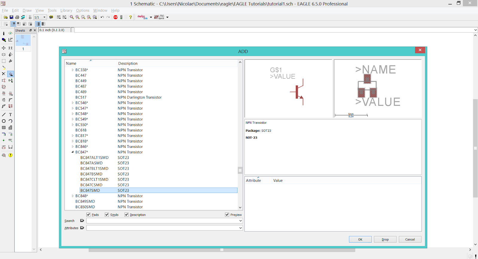
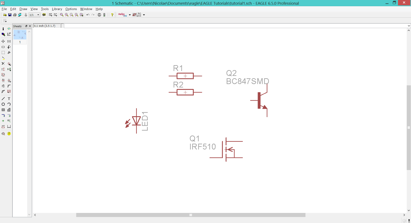
The NPN transistor is to be found in transistor-npn.lbr > BC847* > BC847SMD. Add one on the workspace.

EAGLE CAD - Transistor-NPN Library

EAGLE CAD - Placing The NPN Transistor

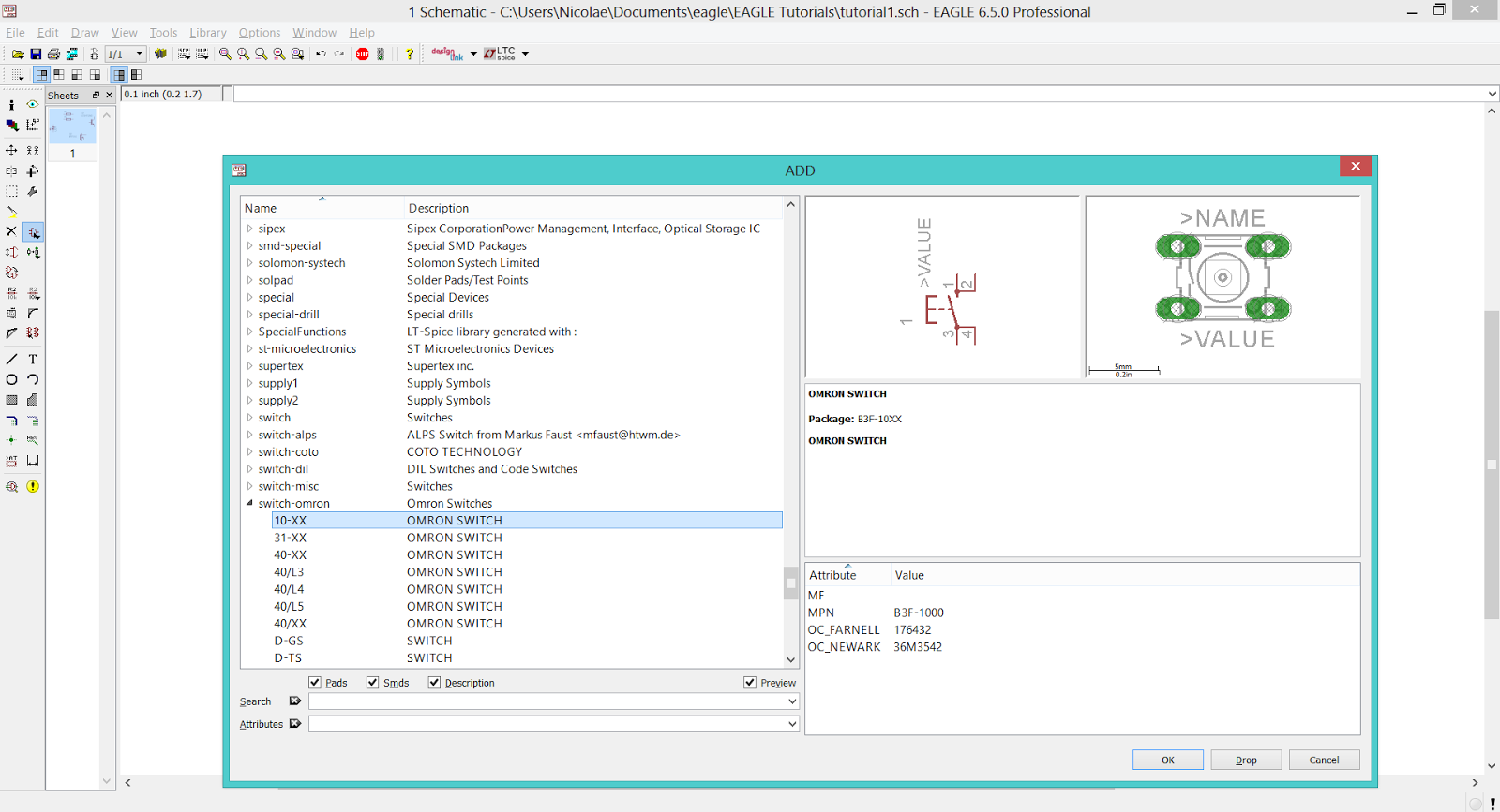
Add the push-button from switch-omron.lbr > 10-XX.

EAGLE CAD - Switch-Omron Library

EAGLE CAD - Placing The Push-Button

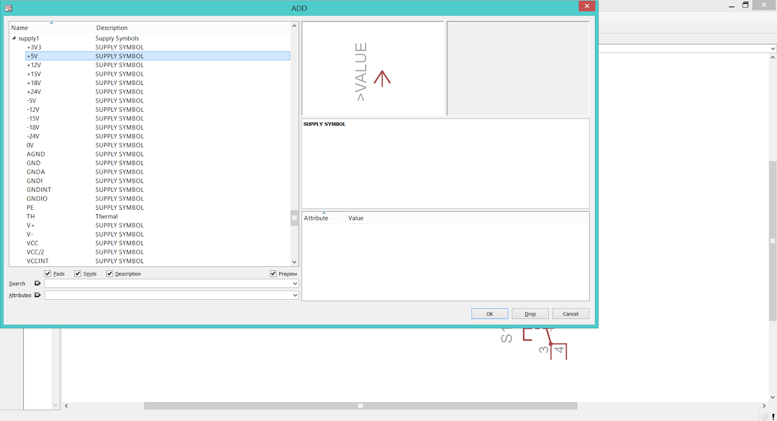
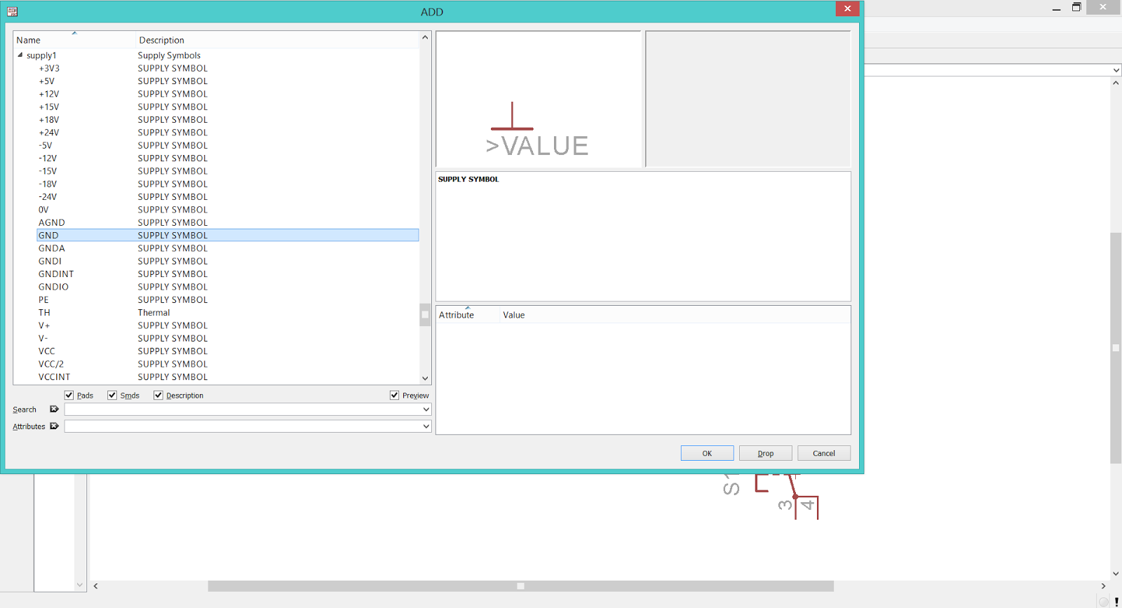
Finally, add the power rails from supply1.lbr > +5V and supply1.lbr > GND.

EAGLE CAD - Supply1 Library (+5V)

EAGLE CAD - Supply1 Library (GND)

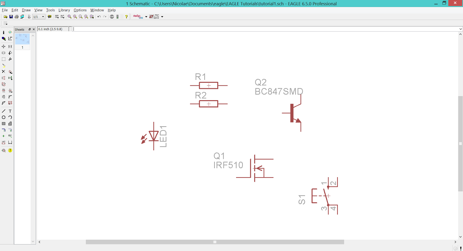
EAGLE CAD - Placing The Power Symbols

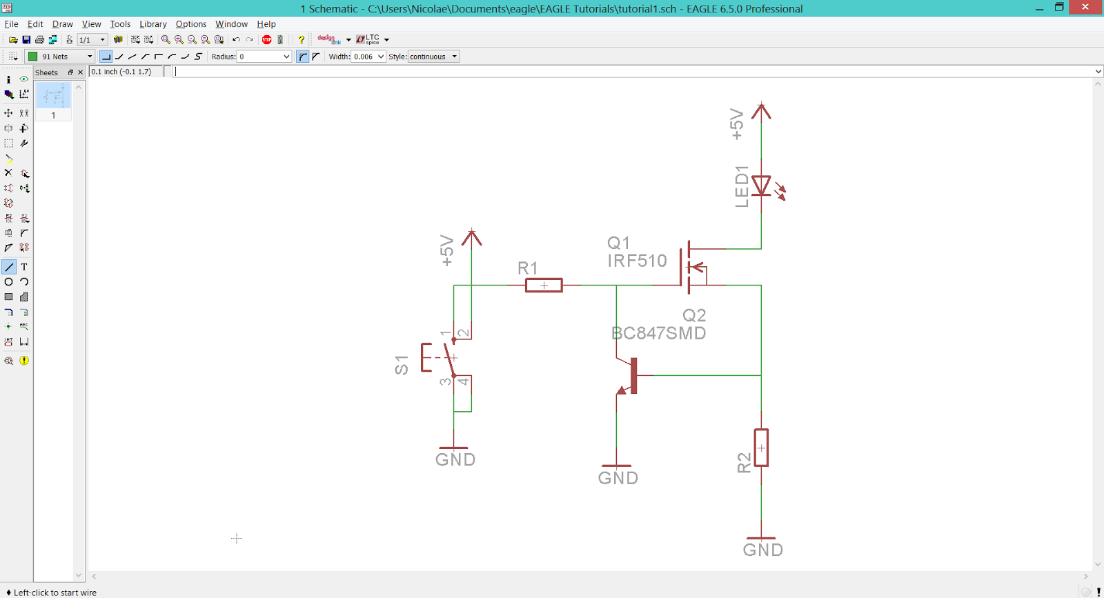
Now we have all the needed components on the workspace, so we can put them in the right order and connect them with the Wire Tool.

EAGLE CAD - Using The Wire Tool To Connect The Devices Together

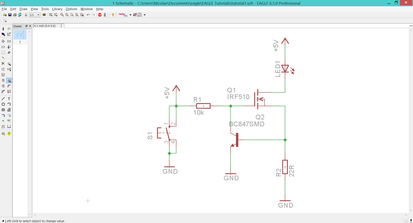
Don't forget to place junctions (using Junction Tool) and give values to the devices (using Value Tool).

EAGLE CAD - Place Junctions And Give Values To The Devices

We're ready! The first schematic is up on her way to become a PCB. For a more 'easy to understand' version of this guide, check the following video (coming soon).